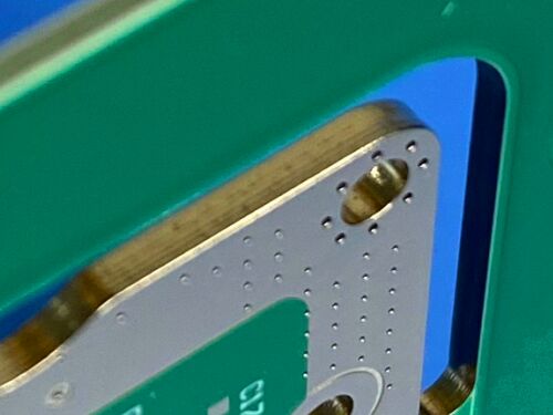
このPCBは8層の銅構造で,高性能素材の組み合わせと厳格な製造基準を採用し,高い信頼性の電子アプリケーションの要件を満たしています.樹脂で満たされたキャップバイアス,エッジプレート (金属エッジラッピング),浸し金表面仕上げ,白いシルクスクリーンで緑色溶接マスク,優れた信号完整性,熱性能,機械的な強さを保証します.
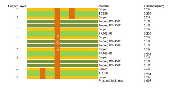
PCBコア仕様
| 建設パラメータ |
仕様 |
| 基礎材料 |
TC350,FR408HR,RO4450F プレプレグ |
| 銅層数 |
8層 |
| 銅の重量 |
1層あたり1オンス |
| 完成板の厚さ |
2.0mm |
| 板の寸法 |
99mm × 83mm |
| 表面塗装 |
浸水金 (ENIG) |
| 溶接マスク & シルクスクリーン |
双面:緑色の溶接マスクと白いシルクスクリーン |
| 設定経由で |
ブラインドバイアス,0.2mmバイアス,樹脂で満たし,電圧塗装で覆い (満たし,覆い) |
| 特別 な 特徴 |
縁の塗装 (金属の縁の包装) |

TC350 材料の紹介
TC350繊維ガラスで強化され,セラミックで満たされ,PTFEベースのPCB基板複合材料で,熱伝導性が優れた (1.0W/mK) で,熱伝達を強化する.介電体と挿入損失を減らす, 増幅器/アンテナの増幅と効率を高めます.より高い電力を処理し,ホットスポットを最小限に抑え,限られた熱管理のアプリケーションに適しています.
TC350ラミナットは,高温で優れた介電常定性 (−9ppm/oC) を維持し,電源増幅器,アンテナ,相/阻抗感のあるデバイスにとって極めて重要です.低Z方向CTEは銅とマッチします (プラテッド透孔の信頼性を保証します)"柔らかい基板"として,落下試験基準を満たすために振動/衝撃に耐える.
マイクロ波グレードの低プロファイル銅に強く結合し,高RF/マイクロ波周波数で挿入損失をさらに削減します.伝統的なラミナットよりも掘り易いし,熱力ストレス環境で信頼性の高い銅粘着のために高い剥離強度を持っています..
TC350 主要な特徴と利点
"クラス最高の"熱伝導性 (1.0 W/mK) と,広い温度 (-9 ppm/oC) での電圧不変の安定性
- 非常に低い損失触角,より高いアンプまたはアンテナ効率を提供
- 商業用アプリケーションのコスト効率性
- 厚い密集した織物ガラスで従来の商業用ラミナットよりも簡単に掘り出せる
- 熱力応変用での信頼性の高い銅粘着のために高い皮質強度
- 優れた熱散と熱管理能力
- 処理効率と全体的な信頼性の向上
- 処理コストを削減するために複数の回路のレイアウトを可能にする大きなパネルサイズで利用可能
TC350 典型的な用途
- 電源増幅器,フィルター,カップラー
-タワーマウントアンプ (TMA) とタワーマウントブースター (TMB)
- 熱循環型アンテナ 介電漂流に敏感
- マイクロ波コンビナーとパワーディバイダー
FR408HR材料の紹介
FR408HRは高性能FR-4樹脂システムで,ガラスの移行温度 (Tg) は230°C (DMA) である.熱性能と信頼性が最大限要求される多層PCBアプリケーション用に特別に設計されているISOLAの特許のある高性能多機能樹脂システムで製造され 電気グレード (Eガラス) のガラス繊維で強化されていますFR408HRは,Z軸の拡張を30%改善し,同カテゴリーの競合製品と比較して25%の電気帯域幅 (低損失) を提供しています.
FR408HRはレーザー発光とUV遮断で,自動光学検査 (AOI) システムとの最大限の互換性を確保する標準FR-4製造プロセスと優れた処理互換性を提供します.既存の生産ラインに簡単に組み込める.
FR408HR 典型的な用途
- 高熱性能と信頼性を要求する多層PCB
- 鉛のない組み立てアプリケーション
- 密集した部品レイアウト (ピッチ容量0.8mm) を有する電子機器
-AOI互換性と精密な溶接マスクイメージングを必要とするPCB
- 複数のリフローサイクルの高い信頼性の電子システム
バイア・フィール・アンド・キャップ (レジン・フィール・アンド・エレクトロプレート・キャップ) とは?
Via filled and capped (バイアス・フィール・アンド・キャップ) は,バイアスの信頼性と性能を向上させるために設計されたPCB製造プロセスです.特に高密度でこのプロセスは,樹脂の詰め込みと電圧塗装の蓋を2つの主要なステップで構成します.
まず,バイアス (このPCBでは0.2mmの盲目バイアス) は高温耐性のある隔熱樹脂で満たされます.樹脂は穴を通って全体を満たし,空気の隙間や空隙が残らないようにします.水分吸収を阻害する,信号の干渉を軽減し,経路の機械的強度を向上させる.使用された樹脂は,通常PCBラミネーションとリフロー温度と互換性があります.製造過程で安定性を維持する.
樹脂を固めた後,2つ目のステップ"電圧塗装蓋"が行われます.PCBの表面仕上げに一致する) は,樹脂で満たされた表面に電圧塗装されます.このキャップは,組み立て中に損傷から樹脂を保護し,電気連続性を確保します (必要に応じて),部品の取り付けに平らな表面を備える高密度のPCB設計において 極めて重要です
詰め込みのメリットには: 組み立て中にビアスに溶接器が入り込むのを防ぐこと,高速アプリケーションでの信号反射とクロスストークを減らすこと,熱伝導性を向上させる環境要因 (湿気,塵) から保護し,PCBの全体的な機械的な強さを向上させる.
エッジ プレート の 役割
エッジプラチング (Edge Plating) とは,金属エッジラッピングとも呼ばれるPCB製造プロセスで,PCBの露出したエッジを導電性金属 (通常は銅,このケースでは,PCBの浸水金と同じ表面仕上げが続く)このプロセスは,PCBの性能,信頼性,製造能力を向上させる上で重要な役割を果たし,以下の主要な機能があります.
改善された接地とEMIシールド: エッジプラチングは連続的な伝導回りを形成し (ファラデーケージ),接地完整性を向上させ,外部EMIを削減します.高速道路では非常に重要です.信号の完整性を要求するRFおよびマイクロ波アプリケーション
強化された機械的強度:PCBの機械的強さを高め,取り扱い,組み立て,操作中に縁の破片,裂け目,損傷に抵抗する特に厳しい環境や高ストレス環境に適しています.
熱散の改善:追加の熱経路として,部品熱を散布し,熱管理を最適化し,結合温度を低下させ,部品寿命を延長します.
便利な電気連続性: 層間の電気連続性を可能にし,接地設計を簡素化し,一貫したパフォーマンスを確保し,信号の整合性を向上させるためにエッジ抵抗を軽減します.
溶接しやすさと組み立ての向上: 滑らかな導電性表面により,端に搭載されたコンポーネント/コネクタの溶接が容易になり,組み立ての信頼性が向上し,溶接関節の故障リスクを軽減します.

 メッセージは20〜3,000文字にする必要があります。
 Japanese