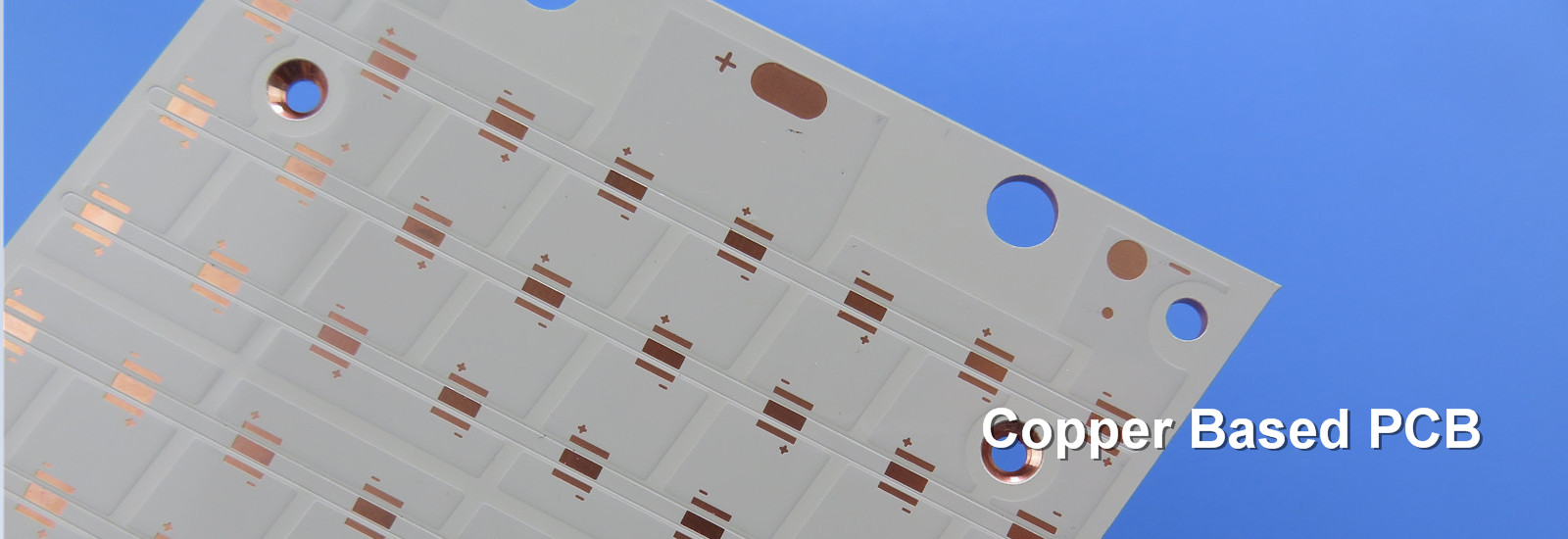

選択するPCB材料:金属コーティングラミネート vs FR-4?
2025-12-18
メタルクラッドラミネートとFR-4 は、エレクトロニクス業界でプリント基板(PCB)に使用される2つの一般的な基板材料です。材料組成、性能特性、および用途分野が異なります。
メタルクラッドラミネートとFR-4の分析
メタルクラッドラミネート: これは、通常アルミニウムまたは銅を金属ベースとするPCB材料です。主な特徴は、優れた熱伝導率と放熱能力であり、LED照明やパワーコンバーターなど、高い熱伝導率を必要とする用途で非常に人気があります。金属ベースは、PCB上のホットスポットから基板全体に熱を効果的に伝達し、熱の蓄積を減らし、デバイスの全体的な性能を向上させます。
FR-4: FR-4は、ガラス繊維布を補強材、エポキシ樹脂をバインダーとして使用するラミネート材料です。これは最も広く使用されているPCB基板であり、優れた機械的強度、電気絶縁特性、および難燃性特性が評価され、さまざまな電子製品に適しています。FR-4はUL94 V-0の難燃性評価を受けており、炎にさらされても非常に短時間しか燃焼しないため、高い安全要件を持つ電子デバイスに適しています。
メタルクラッドラミネートとFR-4の主な違い
1. ベース材料: メタルクラッドラミネートは金属(アルミニウムまたは銅など)をベースとして使用し、FR-4はガラス繊維布とエポキシ樹脂を使用します。
2. 熱伝導率: メタルクラッドラミネートは、FR-4よりも著しく高い熱伝導率を持ち、効果的な放熱を必要とする用途に適しています。
3. 重量と厚さ: メタルクラッドラミネートは、一般的にFR-4よりも重く、薄い場合があります。
4. 加工性: FR-4は加工が容易で、複雑な多層PCB設計に適していますが、メタルクラッドラミネートは加工がより困難ですが、単層または単純な多層設計に最適です。
5. コスト: メタルクラッドラミネートは、金属のコストが高いため、通常FR-4よりも高価です。
6. 用途分野: メタルクラッドラミネートは、パワーエレクトロニクスやLED照明など、優れた放熱を必要とする電子デバイスに主に使用されます。FR-4はより汎用性が高く、ほとんどの標準的な電子デバイスおよび多層PCB設計に適しています。
要約すると、メタルクラッドラミネートとFR-4の選択は、主に製品の熱管理要件、設計の複雑さ、コスト予算、および安全性の考慮事項によって異なります。JDB PCBは、製品の特定のニーズに基づいて材料を選択することを推奨しており、最も高度な材料が必ずしも最も適しているとは限りません。
------------------------------
著作権表示:上記のテキストと画像の著作権は、元の著作者に帰属します。Bicheng はこれを再投稿として共有しています。著作権に関する懸念がある場合は、ご連絡ください。コンテンツを削除します。
もっと見る
2025年には中国本土のPCB(プリント基板)生産額が世界1位となり、シェアは37.6%に上昇する見込みです。
2025-12-18
AIの需要は,印刷回路板 (PCB) の生産と新しい製造拠点の開発に グローバルな拡大を促しています.中国の製造業者は積極的にタイに存在を確立しています韓国のPCB企業は,ベトナムにおけるサムスンの長年の事業を活用し,近年,マレーシアをIC基板の重要な拡大拠点にしました.日本は先進的なパッケージングと高級PCBの生態系を強化するために投資を増やしている台湾のPCBメーカーが"中国プラスワン"戦略を策定し,生産拡大の新たな波を形作りました.
12月14日に the Taiwan Printed Circuit Association (TPCA) and the Industrial Technology Research Institute's Industrial Economics and Knowledge Center released the "2025 Mainland China PCB Industry Dynamic Observation" and the "2025 Japan and South Korea PCB Industry Observation" reportsAIの時代における東アジアのPCB生産基地における産業変化と新しい場所への拡大を分析した.
TPCAは,中国本土が世界最大のPCB生産基地であることを指摘しました. 2025年には,中国本土企業の生産価値が3418億ドルに達すると予想されています.年比22%増加世界市場シェアは37.6%に上昇し,爆発的な成長勢いを示しています.
中国本土の製造業者は 海外への展開を積極的に推進しています タイは有利な投資環境と 発展したインフラを備えています中国本土のPCBメーカーによる生産能力移転の好ましい目的地になりましたTPCAは,中国本土が資金提供するタイのPCB工場の現在の推定生産価値は,総生産価値の約1.7%を占めていると述べた.短期的には 困難に直面するかもしれませんがグローバル化戦略は,地政学的リスクを緩和し,長期的には新しい顧客と市場シェアを吸引することができます..
台湾 (中国) は,世界第2位のPCB生産拠点である.中国本土はかつて台湾のPCB企業の主要生産拠点であった.近年,地政学的リスクの影響を受け,台湾企業は次々と"中国+1"戦略を開始台湾と東南アジアに新しい拠点を設立している.現在,台湾が資金提供している10社以上のPCB会社,Compeq,Zhen Ding Technology,Unimicron,Chin-Poon,そしてゴールド回路電子機器トリポッドはベトナムに重点を置く一方,HannStar BoardとGBMはPSAグループに属し,マレーシアを工場に選んだ..
TPCAは,台湾 (中国) の半導体およびPCB産業は,世界のAIサーバーサプライチェーンにおいて重要な役割を果たしていると述べた.台湾 (中国) は,先端包装の能力の深化と強化を加速する必要がある.AIの時代におけるサプライチェーン再構築における重要な役割を維持するために,地政学的リスクと市場リスクを管理しながら,高級技術と材料の自律性を維持する.
日本は世界第3位のPCB生産拠点である.TPCAは,2024年に日本が資金提供する企業の生産価値が約1153億ドルで,世界の市場シェアは約14%であることを指摘した.4%日本PCB産業は2025年に肯定的な成長に戻ると推定され,国内外総生産額は1182億ドルに上昇し12ドルに達すると予想されています.2026年には35億ドル.
さらにTPCAは,日本が生産能力を高めるために企業投資に頼るだけでなく,AIと半導体に関する政府の最近の国家戦略に準拠していることを示しました制度化された補助金,専用の資金提供システム,そしてサプライチェーンセキュリティ戦略を通じて日本は,先進的な包装と高級PCBエコシステムにおける全体的な競争力を向上させることを目指しています.
韓国は世界PCB市場で4位.TPCAは2024年に韓国の資金提供企業による国内外総生産額が約78億8000万ドルであったと報告した.9 について説明します韓国産業は2025年から2026年まで安定して穏やかな成長を遂げ,総生産額はそれぞれ7940億ドルと816億ドルと予測される..
TPCAは,海外への展開に関して,韓国製PCB企業は,長年にわたりベトナムにおけるサムスンの確立されたサプライチェーンから利益を得て,近年,マレーシアはIC基板の主要な拡大拠点となりました将来のメモリ市場の需要を満たすためにBT基板の容量を積極的に増やす. TPCA analyzed that South Korea will continue to play a significant role in memory and server platforms and maintain its strategic position in the global PCB supply chain through high-end substrate technology.
ほら ほら源:TPCA著作権の通知:上記のテキストと画像の著作権は,オリジナルの著者に属します. 私たちはこれを再投稿として共有しています.著作権に関する懸念がある場合は,私たちと連絡してください.内容を削除します..
もっと見る
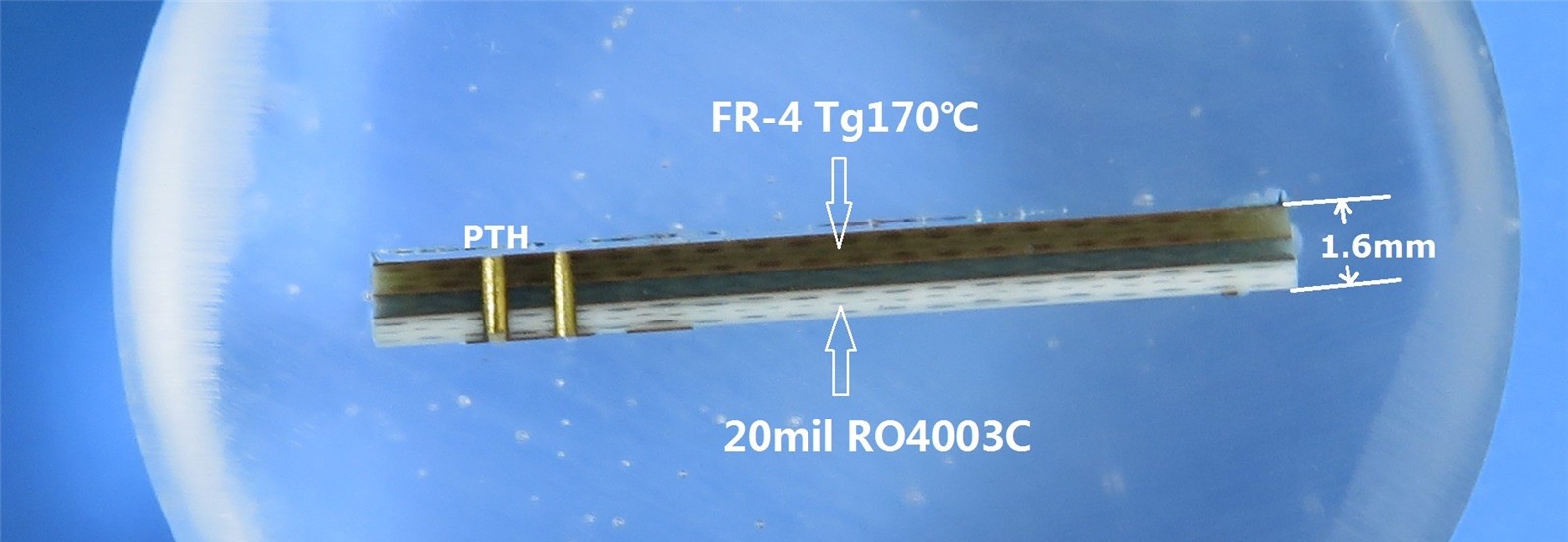
RO4003C LoProラミネートは、RF PCBの性能をどのように向上させるのか
2025-12-03
ラジオ周波数 (RF) と高速デジタル回路の性能は,印刷回路板 (PCB) の基板材料と構造と密接に関連している. The presented board exemplifies how advanced hydrocarbon ceramic materials can be leveraged to achieve superior signal integrity and thermal performance while maintaining compatibility with standard PCB processing techniques.
1紹介
通信・コンピューティングシステムの動作周波数が増加するにつれて,PCB基板の電気特性がシステムの性能に支配的な要因になります.伝統的なFR-4材料は,マイクロ波周波数で過度の損失と不安定な介電常数を示しますこの技術分析は,ロジャーズ・コーポレーションのRO4003C LoProシリーズを使用した具体的な実装に焦点を当てています.高周波性能の最適なバランスを確保するために設計された材料熱管理や製造可能性
2材料選択:RO4003C ロプロラミネート
設計の中心は,炭化水素セラミック複合物であるRO4003Cロプロラミネートである.その選択はいくつかの主要な特徴によって正当化されている:
安定した電解常数: 10GHzで 3.38 ± 0.05 の厳格な許容度は,全体で予測可能なインピーデンス制御を保証し,環境条件の変動に伴います.
低分散因子: 0で0027この材料は, 40 GHz を超えたアプリケーションで信号強度と完整性を維持するために不可欠な電解負荷を最小限に抑える.
熱性能向上: このラミネートは,高熱伝導性0.64W/m/K,ガラス移行温度 (Tg) が280°Cを超えている.鉛のない組み立てや高出力運用環境での信頼性の確保.
低プロフィール銅: "LoPro"という名称は,逆処理されたフィルムを使用することを指し,より滑らかな導体表面を作り出す.これは導体損失と分散を減らす.標準の電極化銅製フィルムと比較して直接挿入損失を改善する.
RO4003C材料システムの重要な利点は,標準FR-4多層ラミネーションと加工手順との互換性です.費用のかかる事前処理の必要性をなくし,その結果,全体的な製造コストと複雑さを削減する.
3PCB 製造と積み重ね
板は2層の硬い構造で,次の詳細なスタックアップがあります.
レイヤ1: 35μm (1オンス) のローリング銅製フィルム.
ダイレクトリック: ロジャースRO4003C ロプロコア 0.526mm (20.7ml) 厚さ
層2 35μm (1オンス) のローリング銅製フィルム.
完成板の厚さは0.65mmで,コンパクトな組立物に適した薄型プロフィール構造を示しています. 構造の詳細は,高い出力と性能のために最適化された設計を反映しています:
重要な次元: 最小の痕跡/空間は5/5ミリであり,最小の穴の大きさは0.3ミリであり,適度なルート密度に対応しながら容易に達成可能な設計規則を示している.
表面塗装: 銀底層の表記は,金底層 (しばしば"硬い"または"電解金"と呼ばれる) がRF設計を示す.この仕上げは,高周波の電流に優れた表面伝導性を提供します低接触抵抗と優れた環境耐久性
ストラクチャを通して このボードは,プレート厚さ20μmの39の透孔バイアスを利用し,インターレイヤ接続の高い信頼性を保証する.盲目バイアスの欠如は製造プロセスを簡素化する.
4品質と基準
PCBのレイアウトデータは Gerber RS-274-X 形式で提供され,製造者への正確なかつ曖昧なデータ転送が保証されました.ボードは IPC-A-600 クラス 2 規格で製造され試験されました.寿命と性能が延長される場合の商業用および産業用電子機器の典型的な基準です.
品質保証 製造後100%の電気テストが行われ,すべての接続の整合性,短パンや開口がないことを確認しました.
5. アプリケーション プロフィール
材料の特性と構造の詳細の組み合わせにより,PCBは以下を含む様々な高性能アプリケーションに適しています.
低パシブインターモジュレーション (PIM) が不可欠なセルラーベースステーションアンテナとパワーアンプ
衛星受信システムにおける低騒音ブロックダウンコンバーター (LNB)
高速デジタルインフラストラクチャにおける重要な信号経路,例えばサーバーバックプレーンやネットワークルーター.
高周波RF識別タグ (RFID)
6結論
分析されたPCBは,ロジャースRO4003Cロープロラミネートの有効な適用の実用的なケース研究として機能します. このデザインは,材料の安定した電気特性,低損失プロファイル,現代の高周波回路の要求を満たすための優れた熱特性さらに,製造仕様では,異国的な製造方法や高額な製造方法を使わずに,このような高い性能を達成することが示されています.
もっと見る
TLX-8 PCBはあなたの高周波アプリケーションに最適な選択肢ですか
2025-12-01
RFおよびマイクロ波設計という厳しい世界において、プリント基板(PCB)は単なる相互接続プラットフォーム以上の存在であり、システムの性能を左右する不可欠なコンポーネントです。材料の選択、スタックアップ、製造公差は、信号の完全性、熱管理、長期的な信頼性に直接影響します。
本日は、特定の高性能PCBの構築を分解し、材料科学と精密製造がどのように融合して、航空宇宙、防衛、通信アプリケーションの厳しい要求に応えているかを示します。
設計図:高周波2層基板
まず、主要な構造の詳細から始めましょう。
ベース材料: Taconic TLX-8
層数: 2層
基板寸法: 25mm x 71mm(±0.15mm)
重要な製造公差:
表面処理: 浸漬金(ENIG)
品質基準: IPC-Class-2
試験: 100%電気試験
これは標準的なFR-4基板ではありません。PTFEグラスファイバー複合材であるTLX-8の選択は、電気的性能が不可欠なアプリケーションであることを即座に示しています。
なぜTLX-8なのか?戦略的コンポーネントとしての基板
TLX-8は、優れた電気的特性と卓越した機械的堅牢性を兼ね備えた、主要な高容量アンテナ材料です。その価値提案は、過酷な動作環境におけるその汎用性にあります。
クリープと振動に対する耐性: ロケット打ち上げ時など、極端な力がかかるハウジングにボルトで固定される構造に不可欠です。
高温性能: 分解温度(Td)が 535℃を超えているため、エンジンモジュールやその他の高温環境での暴露に耐えることができます。
耐放射線性および低アウトガス: NASAが認める、宇宙搭載電子機器に必須の特性です。
寸法安定性: ベーク後の値が 0.06 mm/m と低いため、熱応力下でも一貫したレジストレーションとインピーダンス制御を保証します。
電気的および機械的利点の解読
TLX-8のデータシートの特性は、RFエンジニアにとって魅力的な物語を語っています。
低く安定した誘電率(Dk): 2.55 ± 0.04 @ 10 GHz。この厳しい公差は、基板全体および製造バッチ全体で、予測可能な伝搬速度と一貫したインピーダンス整合に不可欠です。
超低損失係数(Df): 0.0018 @ 10 GHz。これは、信号損失を最小限に抑えることを意味し、高周波および低ノイズアプリケーションに最適です。
優れた受動相互変調(PIM)性能: 通常、 -160 dBc以下で測定され、不要な信号がネットワーク容量を低下させる可能性がある、最新のセルラーインフラストラクチャおよびアンテナシステムにとって重要な性能指標です。
優れた熱的および化学的特性:
スタックアップと製造上の選択肢の分析
シンプルな2層スタックアップは、この低コンポーネント数の設計にエレガントで効果的です。
銅(35μm)| TLX-8コア(0.787mm)| 銅(35μm)
主な製造上の注意点:
ソルダーマスクまたはボトムシルクスクリーンなし: これは、ラミネート自体が伝送媒体を形成し、追加の材料が電磁界に影響を与え、損失を発生させる可能性があるRF基板では一般的です。
浸漬金(ENIG)表面処理: ファインピッチコンポーネントに最適で、必要に応じて信頼性の高いワイヤーボンディングに最適な、優れた耐酸化性を備えた平坦で半田付け可能な表面を提供します。
11コンポーネント基板に27個のスルーホール: これは、グラウンディング、シールド、および熱管理が最重要事項である設計を示しています。堅牢な 20μmビアめっき は、信頼性を保証します。
一般的なアプリケーション:この技術が優れている場所
この特定の材料と製造の組み合わせは、以下の重要な機能に合わせて調整されています。
レーダーシステム (自動車、航空宇宙、防衛用)
5G/6Gモバイル通信インフラストラクチャ
マイクロ波試験装置および伝送デバイス
重要なRFコンポーネント: カプラー、電力分配器/合成器、低ノイズ増幅器、およびアンテナ。
結論:精密工学の証
Taconic TLX-8を選択し、厳しい製造公差を遵守することにより、この構造は、標準的な材料では達成できない、高周波性能、卓越した信頼性、および環境耐性の組み合わせを実現しています。これは、高度な電子機器において、基盤、つまりPCB自体が、システムの成功において積極的かつ決定的な要素であることを強調しています。
もっと見る
AI需要がサプライチェーンに連鎖反応を引き起こし、CCL業界は「量と価格が共に上昇」
2025-11-25
AIコンピューティングパワー革命は、ハイエンドプリント基板(PCB)の需要を急増させ、その上流の主要基材である銅張積層板(CCL)に構造的な成長機会を生み出しています。一部の高品質カテゴリーは、ホットな商品となっています。国内CCL工場の関係者は、「今年の最初の半年で需要は回復しましたが、需要に供給が追いつかないかどうかは製品によります。一部の製品には非常に強い需要がありますが、他の製品は着実な成長を経験しています」と述べています。複数のインタビューを通じて、CLS記者は最近、多くのCCL企業が今年中に製品価格を数回引き上げており、動的な調整がまだ進行中であることを知りました。コスト圧力と需要配当が、価格上昇の主な要因です。高周波・高速CCLや高熱伝導CCLなどのハイエンド製品の将来的な成長可能性に楽観的であり、国内メーカーも関連する能力のレイアウトを加速させています。
CCLがPCBのコスト構造の大部分を占めており、CCLの主要な原材料である銅箔がコストの30%以上を占めていることが理解されています。銅価格の上昇は、CCLの製造コストに直接影響します。国際的な銅価格は今年に入っても上昇を続け、LME銅は10月末までに1トンあたり11,200ドルという高値をつけました。高銅価格の主な理由について、卓創情報の分析担当者である唐志豪氏は、CLS記者のインタビューで、AIコンピューティングセンター、チップ用銅箔、グリッドアップグレードが銅消費を牽引していると述べています。中国の新エネルギーおよび電力部門は高い繁栄を維持しており、不動産不況からの影響を相殺し、低在庫が価格弾力性を増幅させています。「今後、鉱山のグレードの低下と深層採掘により、持続的なCAPEXが継続的に上昇するでしょう。2025年から2030年までの鉱山生産の年平均成長率は約1.5%にとどまると推定されており、需要成長率をはるかに下回っています。供給不足の予想は、銅価格を強く支えるでしょう」と唐志豪氏は考えています。短中期的に、LME銅の主要な取引レンジは1トンあたり10,000ドルから11,000ドルです。中長期的に、鉱山側の投資が依然として遅れており、グリーン需要が予想を上回る場合、平均価格は徐々に1トンあたり10,750ドルから11,200ドルに上昇すると予想されます。
消費者側では、一部の銅を使用する企業が、銅価格の上昇に対処するためにヘッジオペレーションを実施しています。他の企業はより直接的で、シート材料の価格を引き上げることでコストを転嫁しています。今年の最初の半年だけで、「銅価格の急騰」により、大手メーカーであるKingboard Laminates(01888.HK)は3月と5月に価格引き上げ通知を発行し、業界の他のメーカーもそれに追随しました。
価格引き上げはコストだけでなく、需要側の構造的な成長もCCL製品の価格上昇に貢献しています。「PCBは、下流の需要に応じて常に更新される成熟した製造業です。市場の変化は速く、需要も速く、材料サプライヤーとして、私たちもそれに応じて変化しなければなりません」と、業界関係者はCLSに語り、さらに「AIコンピューティングパワー、ロボット工学、ドローン、新エネルギー車の電子制御システムはすべてCCLと回路基板を必要とし、使用量は比較的多い」と付け加えました。
CLS記者は最近、投資家を装って上場CCL企業に電話をかけました。南亜新材料(688519.SH)の証券部門の担当者は、現在の稼働率は90%を超えていると述べました。価格はすでに上昇しており、引き上げのタイミングについては、「10月に引き上げがありました」と明らかにしました。さらに、今年の最初の半年にも価格引き上げがありました。華正新材料(603186.SH)の担当者も、現在の稼働率は高く、今年の最初の半年と昨年と比較して増加していると述べました。価格引き上げについて、彼らは「対応する調整を行っています。10月に調整を開始し、製品と顧客に基づいて動的な調整を行っています」と述べました。銅価格の高騰により製品価格が調整されるかどうかについては、担当者は原材料価格の上昇の程度と持続可能性を総合的に考慮する必要があると示唆しました。金安国紀(002636.SZ)の担当者は、同社の価格設定は市場に従っており、価格と需要は互いに補完し合っていると述べました。製品価格は、市場の需要が強い場合にのみ上昇する可能性があります。
さらに、一部の業界メーカーは、さまざまなCCL製品の価格をバッチで調整していると述べています。国内CCL工場の関係者はCLS記者に対し、市場全体の需要は増加していると語りました。同社の売上高は、2023年と2024年に2桁の年間成長率を維持しました。売上高は増加しましたが、以前の低価格のため、収益性は低く、非GAAPベースの純利益は依然として赤字でした。国内競争は激しく、下流のプレーヤーは独自のコスト要件を持っているため、上流の材料が高すぎることはできず、CCL価格が非常に安定することを妨げています。関係者は、CCL製品の価格が2022年に下落し始め、昨年まで続いたことを認めました。現在は回復していますが、2021年に見られたレベルには程遠いです。
しかし、市場状況のさらなる改善と、以前の価格引き上げからの恩恵により、メーカーの業績は大幅に向上しました。今年の最初の3四半期で、深セン科技(600183.SH)、金安国紀(002636.SZ)、超音波電子(000823.SZ)などの業界企業は、売上高と純利益の両方で成長を達成し、純利益はそれぞれ20%から78%増加しました。業績の変化について、金安国紀は第3四半期報告書で、主に主力製品の粗利益が増加したためであると指摘しました。
AIサーバーなどのアプリケーションシナリオにおける高品質CCLの需要が高まるにつれて、国内メーカーもM6グレード以上の製品の技術レイアウトを加速させています。たとえば、深セン科技の超低損失製品はすでに大量供給されており、超英電子(603175.SH)はインタラクティブプラットフォームで、同社がM9 CCL技術について複数の顧客と緊密に協力していることを明らかにしました。南亜新材料のゼネラルマネージャーである包新陽氏は最近、決算説明会で、高速材料分野において、同社がM10グレードCCL製品の研究開発レイアウトを積極的に開始したと述べました。次世代製品の技術的な焦点は、信号伝送品質をさらに向上させるためのさらに低い誘電損失の達成、パッケージング相互接続の信頼性を向上させるための低い熱膨張係数(CTE)、および高まる放熱需要に対応するためのより高い耐熱性の達成にあります。M10グレードCCL製品の進捗状況について、同社の証券部門の担当者は、「ラボ製品はすでに出ています」と述べました。
産業研究は、AI CCLが新たな業界成長の原動力になると考えています。彼らの推定によると、AI CCL市場(AIサーバー、スイッチ、光モジュール向け)は2025年に22億ドルに達し、前年比100%の増加となります。2026年には、ASICの大量出荷とNVIDIAの新製品がCCLをM9にアップグレードすることにより、AI CCL市場は34億ドルに達し、前年比60%の増加になると推定されています。2028年までに、58億ドルに達すると予想されています。2024年から2028年までのAI CCLの複合年間成長率(CAGR)は52%と予測されています。
---------------------------------
出典:CLS
免責事項:私たちはオリジナリティを尊重し、共有にも重点を置いています。テキストと画像の著作権は元の著者に帰属します。再版の目的は、より多くの情報を共有することであり、このアカウントの立場を表すものではありません。お客様の権利が侵害された場合は、速やかにご連絡ください。できるだけ早く削除いたします。ありがとうございます。
もっと見る